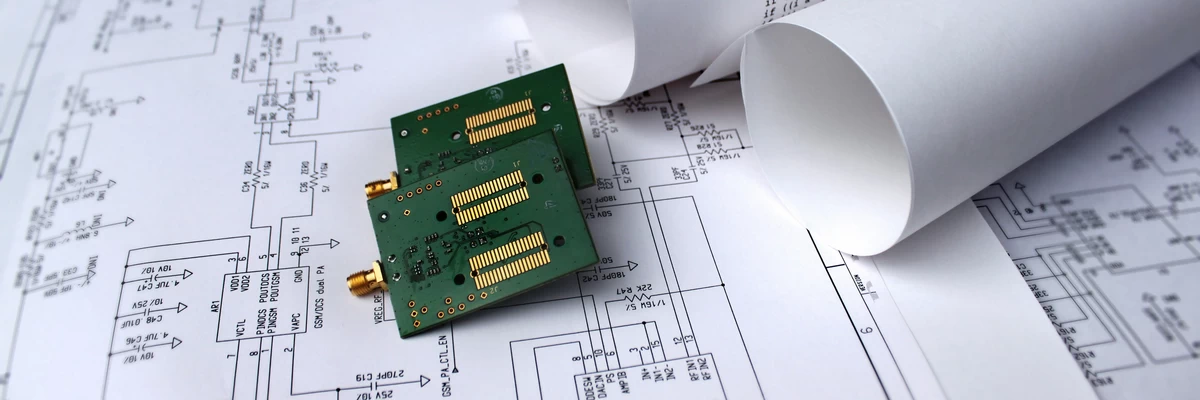
Our dedicated team of PCB professionals will provide you with the most innovative and cost-effective solutions for your front-end design through mass production.
North American customer support together with offshore production facilities, provides our customers the support and pricing required to remain competitive in today’s market.
AGS offers rep opportunities to quality suppliers of products and services in the PCB and electronic component industries. For more information on these opportunities, please contact AGS via this site.
At AGS, we are global experts in designing, engineering, and manufacturing of printed circuit boards. For more than 30 years, we have developed our expertise and worked with clients across different industries to deliver the very best in PCB services. Our own PCB technology experts partner with some of the best PCB manufacturers. Over the years we have been serving our clients, we have built strong relationships with each of our partners. Our team can help with a range of PCB needs, ensuring all of our clients are satisfied with the results that they receive from our services.
Flexible PCBs are used in a variety of different applications such as portable electronics, devices, hard dish drives and desktop printers
Rigid PCBs are designed for applications that have complicated circuit layouts or need many electric components mounted. This type of PCB offers high durability, reliability and a long life cycle, which is why they are often used in LEDs, as well as automotive, medical, HVAC, fitness equipment and industrial applications.
Simply get in touch with us to discuss your requirements. Use our online form to send us your information for a free quote or just to discuss how we can help you. You can also call us directly at 001 256 883 4400 (US) or 86-755-2828 2772 (China) to speak to a PCB specialist and receive more information.
When you get in touch with our expert team, you will receive the best advice on PCB design, manufacturing, assembly, and prototyping. Take a look at our PCB capabilities to see what we can do for you and what we are truly capable of.
Designs to support thru hole and surface mount. Normally used in automotive industry.
Mixed technology circuitry supporting SMT and thru hole.
Typically use thermal dielectric materials bonded to an aluminum core for highly efficient dissipation of heat to cool components and increase the overall performance of products. LED PCBs are the most common usage.
Up to 64 layer PCBs for High speed advanced designs.
High Density Interconnect using laser drilled microvias up to 4-N-4.
Larger and thicker than normal PCBs often with press fit connectors. Used in Telecommunications as backbone interconnections.
Usually made using polymide (Kapton) materials, these are single, double and multilayer(upto8 layers) PCB.
Rigid PCBs with bend areas milled down to make it very thin. They are meant to be bent on installation and not flex afterwards. A much cheaper alternative to PI flex and rigid flex.
Hybrid of Rigid and flex PCBs. The rigid portions are connected by flex imbedded in the inner layers. Although more expensive than rigid PCBs connected by flexible cables, connectors and discrete wiring, they have higher reliability connections.
Rigid PCBs, uses upto 12oz copper layers. Typically used in high power transmission applications.
Aluminium PCBs and embedded copper layers for highly efficient dissipation of heat to cool components and increase the overall performance of devices.
Applications that typically require laminates with specialized electrical, thermal, mechanical, or other performance characteristics that exceed those of traditional standard FR-4. Used for signals that are 5 GHz and higher. Typically using PTFE (Teflon) materials.
Immersion Silver is a good alternative to Electroless Nickel/ Immersion Gold (ENIG) for fine pitch applications due to the lower cost. This finish is becoming a standard in the industry and works well in lead-free processing. Surface preparation is available in polish or etch, it is important to note that polish should be used for micro technology and etch for all others. NOTE: This finish is not backwards compatible with leaded processing and should NOT be selected for applications which will switch between leaded and lead-free.
ENIG is a long proven industry standard and is readily available from most PCB fabricators. This finish is suitable for almost any lead-free application regardless of complexity; however is the highest cost finish. This finish is backwards compatible with both leaded and lead-free processing.
OSP is one of the PCB surface finishes, means Organic Solderability Preservatives, which is applied upon the bare copper to prevent PCB from being oxidized. OSP is RoHS compliant and can be quickly removed in the PCB assembly processing.
Immersion tin is a lead-free surface finish, which is excellent for small components. It is very thin and flat; it is perfect for Fine Pitch Technology (FTP).
Hot air solder leveling (HASL) is a widely used PCB surface finish. It is inexpensive and easily available. It also offers a high solderability finish, making it a dominant player in the market for several years. Due to the RoHS directive, there is a major transition from HASL to lead-free HASL.
Soft gold PCB surface finish that is very well suited to wire bonding operations. The soft gold used in this process can easily form strong metallic bonds with standard copper traces and wires. The strong bond of gold and copper allows for more conductive connections when leads are soldered to the board during the PCB Assembly Process.
ENEPIG is the best surface finish that resists corrosion and reaction with air. It has a longer shelf life, which makes it the best of all.
Plated Gold surface finish is also known as Hard Gold surface finish. It’s an expensive surface finish that uses a layer of gold on the PCB. It’s done through electroplating, and a hard layer of gold is attached to the surface of the copper. The adhesion between the PCB and the layer is firm, which increases the durability of the board.
Soft gold PCB surface finish that is very well suited to wire bonding operations. The soft gold used in this process can easily form strong metallic bonds with standard copper traces and wires.
Design for Fabrication (DFF) is intended to help review customers’ designs with respect to PCB manufacturability as early in the design cycle as possible.
Electrical diagram of the PCB Board.
Design for Manufacturing to improve yields in the assembly process.
Increase the density by using smaller components to reduce overall size of the PCB
Controlling the time it takes for signals to get from one point to another by controlling line with and distance to a copper plane layer.
Have questions or need assistance with our electronics manufacturing services? Our sales or customer service team is here to help. A representative will be in touch within 24 hours.
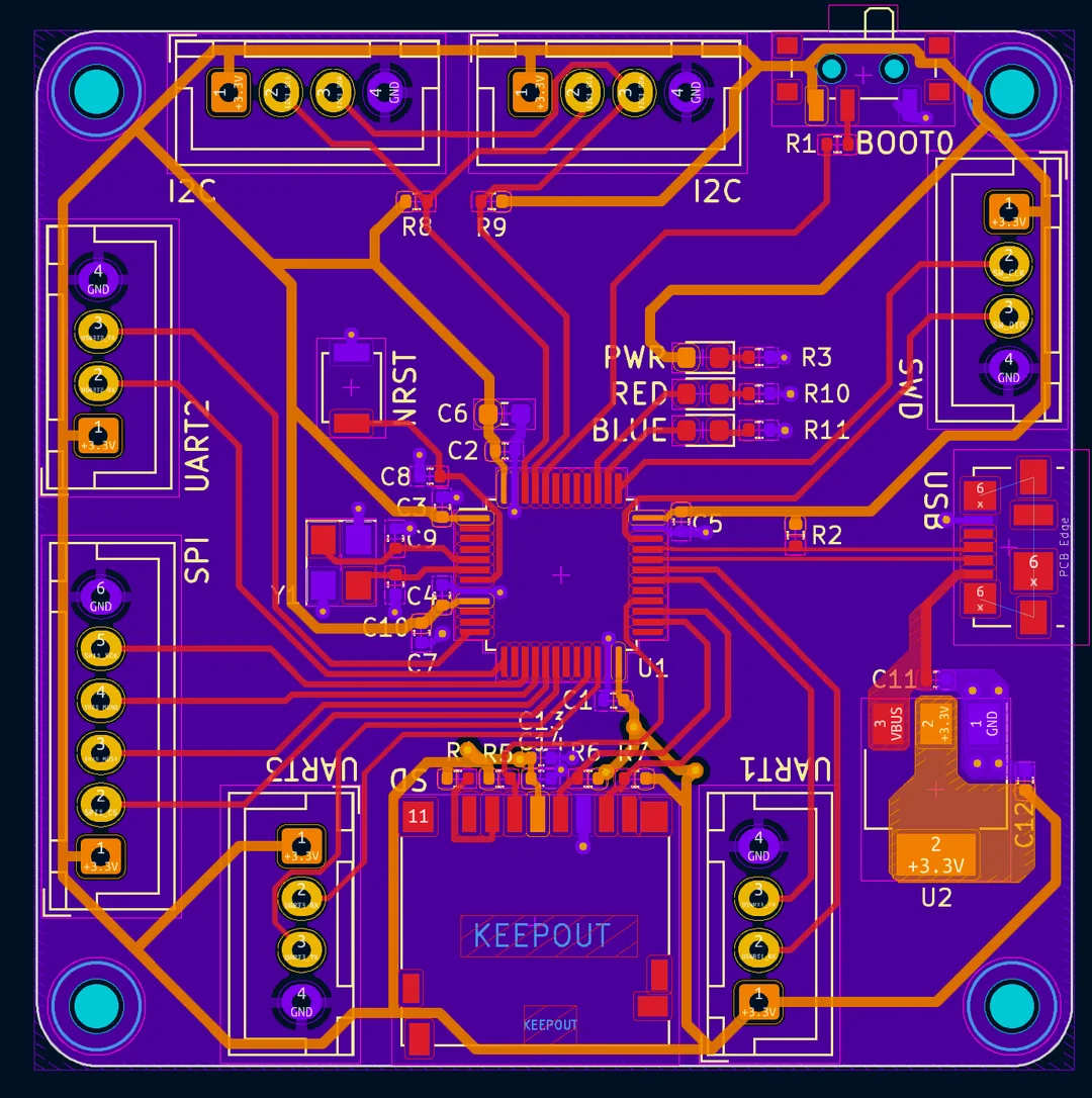
Our Custom Materials Services Team have extensive experience in a wide range of industries and application areas. Our facilities and staff are capable of meeting all kinds of specifications, from simple PCB design to incredibly complex technology. Our team of experts are capable of listening to and understanding the problems that you need to solve, and ensuring the right solution is provided.
We can help with everything from simple circuitry to complex boards that are designed to solve complex problems. Our team collaborates with you to design solutions that are unique to your requirements and use innovative design that works for you. We work closely with you to keep you up to date and guarantee an end result that works for you.
After your PCB design is complete, we also take care of all other PCB assembly manufacturing needs. Our manufacturing partners allow us to provide top-quality PCB prototyping and manufacturing services using the best technology and state-of-the-art facilities. We use design for excellence (DFX) principles, including design for manufacturing (DFM) and design for testability (DFT) to design and review your products. These guidelines and methodologies ensure the product design requirements are met and the product delivers high value to the client. You can be confident that you will receive high-quality design and manufacturing, no matter what industry you need PCB design for.
Creating prototypes is an essential part of the product development process. Our manufacturing services also include prototyping before actual manufacturing and assembly. We offer a fast, complete prototyping service that gives you everything that you need to quickly get your product tested and ready to be manufactured. You can choose Vexos for rapid PCB and PCBA prototyping. We have complete value engineering services, as well as integrated and coordinated technology and components solutions. We manage every project according to ISO standards to guarantee consistently high-quality results every time.
Our prototyping process involves using the latest equipment and process controls, including component kit check-in and final inspection methods. We deliver the highest level of technical service throughout the process. Beginning with receiving your files or completing your design, our team communicates effectively with you throughout the project and provides project management, with a clear focus on quality and delivering your project on time.
Your prototypes can be ready in just a matter of days and you are able to order any amount, beginning with just a single board. We provide a range of board types and different finishes for you to choose from to develop a final prototype that meets your project’s specifications. You can get your product to market faster with our prototyping services, whether you use them as a standalone service or together with our other service options.
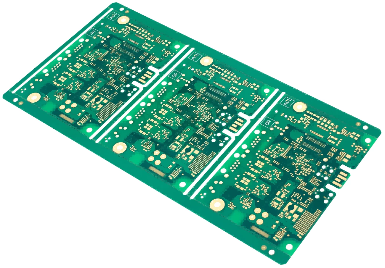
| Item | Standard | Advanced | |
|---|---|---|---|
| PANEL SIZE | Maximum | 600*730 mm ( 24*29 inch) | 650*1120 mm (26*44inch) |
| BOARD THICKNESS | Maximum | 7 mm (0.28 Inch) | 10 mm (.39inch) |
| Minimum | 0.3 mm ( 0.012 inch) | 0.2 mm (0.008 inch) | |
| LAYER COUNT | Maximum layer count rigid boards | 36 | 64 |
| Maximum layer count flex boards | 14 | 20 | |
| LAYER TO LAYER REGISTRATION | minimum missregistration | 0.1 mm ( 4mil) | 0.075 mm (3mil) |
| COPPER THICKNESS (INNER/OUTER LAYERS) | Maximum thickness | 210 micron (6oz) | 420 micron (12oz) |
| MINIMUM CORE THICKNESS | Minimum core thickness | 50 micron (2 mil) | - |
| LINES/SPACES | Minimum outer layer line/space | 75/75 micron (3/3mil) | 50/50 micron (2/2mil) |
| Minimum inner layer line/space | 63.5/63.5 micron (2.5/2.5mil) | 40/40 micron (1.6/1.6 mil) | |
| MECHANICAL DRILLING | Maximum aspect ratio | 1:14 | 1:20 |
| Minimum drill diameter | 0.15 mm (6mil) | 0.1 mm (4mil) | |
| final hole tolerance (PTH) | ± 0.05 mm (± 2 mil) | ±0.038mm (±1.5mil) | |
| LASER DRILLING | Minimum laser diameter | 75 micron (3mil) | 60 micron (2.4 mil) |
| Aspect ratio microvia (Hole size / thickness) | 0.8:1 | 1:1 | |
| IMPEDANCE CONTROL | Accuracy | ± 10% | ± 5% |
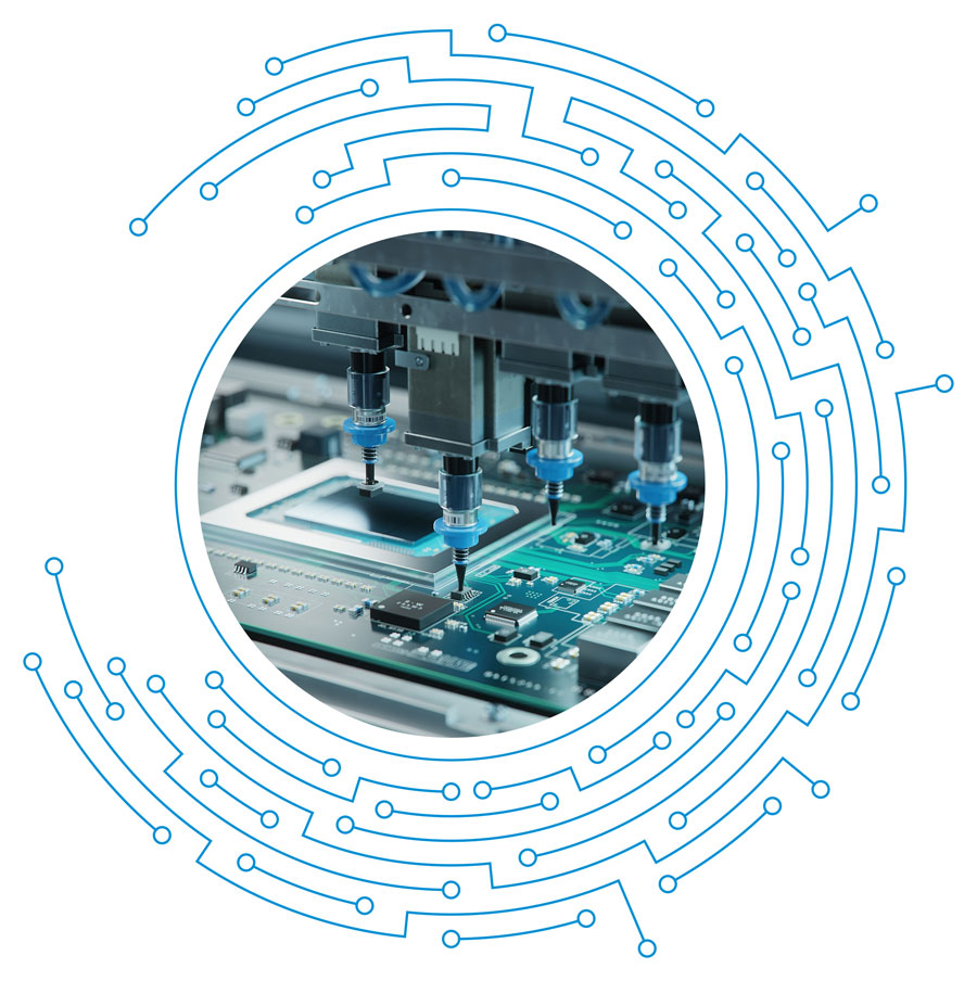
Our PCB manufacturing services ensure our clients are able to take their PCB projects from initial stages to completion phase. Assembly, testing and commodity sourcing are all part of our complete service offering. Vexos partners with the very best manufacturers to enable us to take your PCB from concept through to design and manufacturing. Our fully-equipped facilities have a wide range of capabilities and all assemblies are verified for part-placement accuracy. We choose our subcontractors extremely carefully, using rigorous criteria to ensure we choose only the best partners for PCB manufacturing. Each of our partners is subject to frequent checks and factory visits throughout the manufacturing process, enabling us to have full oversight and guarantee quality results.
Continuous training is provided to staff at all levels to ensure they have updated knowledge and skills needed to deliver excellent quality products. We also prioritize your privacy, keeping careful control over documents and safeguarding your data. Additionally, our manufacturing partners are chosen to help us offer competitive prices to our clients. Together with our design team, we can ensure that your PCBs are ready for manufacturing and designed in a way that makes fast and reliable manufacturing more feasible.
Our global manufacturing capabilities make it possible to provide flexible solutions to all of our clients. All of our facilities have the latest technology and equipment and benefit from custom materials sourcing, logistics, aftermarket services, and more. Whatever your needs are, we can provide the solutions to match them.
Whether you have a standalone PCB fabrication project or you need assistance with design, manufacturing and other requirements, we work with you to get it done. We have all of the necessary quality equipments to fabricate assemble your PCBs and test their function to ensure they are prepared for the next stage of your project.
Our printed circuit board manufacturing and sourcing services make sure you have the key component of your circuit boards. Together with our PCB sourcing assembly services, you can complete the assembled printed circuit board with all of its requisite parts. Both our assembly and testing services prepare your PCBs as part of our one-stop service. We can take care of everything from multi-layered to flexible printed circuit boards, providing services from design to delivery.
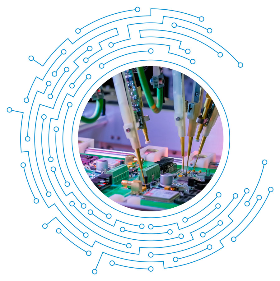
Testing involves checking electrical testing of finished PCBs. Our state-of-the-art equipment ensures a thorough job is carried out every time.
24/7 CUSTOMER SERVICE
Shen Zhen City, China
Mon-Fri: 10:00 - 21:45
Sunday: Closed
CHINA - CARL: +86 136 99888802
US - RON: 256 883 4400
sales@agssales.com
© 2025 AGS Limited All Rights Reserved